


Nanoelectronics and Semiconductor Devices Group
Memristors and Crossbar RRAMs

Memristors have certain unique properties such as state-dependent resistance, non-volatility, and hysteresis behavior with a characteristic pinched I-V loop. These properties make them ideal for analog memory and computation. Unlike traditional binary memory, memristors support multi-level resistance states. This allows multi-bit storage per cell, analog computation, as well as synaptic weight emulation. Their bidirectional conductance change enables spike-timing dependent plasticity (STDP) and Hebbian learning for neuromorphic systems. Importantly, they promise much higher energy efficient than traditional SRAM or DRAM. Their switching energies can be as low as femtojoules. Because of their simple design, they are ideal for 3D crossbar integration, which helps in realizing high-density high-speed memories. All these advantages allow them to be used in applications such as non-volatile memory (NVM), neuromorphic computing, in-memory computing, physical unclonable functions (PUFs), analog signal processing, logic-in-memory etc. Research directions include developing 3D memristor architectures (3D RRAM, HRRAM, VRRAM) for high-density neuromorphic arrays, integrating edge AI processors (e.g., for wearables, smart cameras, IoT), self-healing and bio-inspired circuits, crossbar-based cloud accelerators, flexible and wearable electronics, radiation-hardened memory for space, quantum and stochastic neuromorphic systems etc. Our group currently focuses on developing crossbar RRAMs with emerging materials such as perovskites with high flexibility and endurance.
Solar Photovoltaics
Solar photovoltaics (PV) have emerged as a dominant technology in the global transition to clean energy, with over 1 terawatt of cumulative capacity deployed worldwide. Traditional crystalline silicon solar cells lead the market due to their high efficiency and proven reliability. However, the next generation of PV technologies—including perovskite solar cells, organic photovoltaics (OPVs), and quantum dot solar cells—are rapidly advancing, offering promising alternatives with unique benefits. Among these, ultra-lightweight, flexible, and printable PV materials are gaining attention for specialized and portable applications, such as wearable devices, aerospace, and building-integrated photovoltaics (BIPV). Indoor PV systems are also under active development, particularly for powering low-energy electronics and Internet of Things (IoT) devices under artificial lighting conditions.
Flexible and printable solar cells can be manufactured on substrates like plastic or paper using low-cost roll-to-roll techniques, enabling seamless integration into unconventional surfaces. Despite significant progress, challenges remain—especially in improving long-term operational stability, environmental durability, and scaling up sustainable manufacturing processes. Research efforts are also focusing on plasmonics, tandem cell architectures etc. to surpass efficiency limits, and the use of non-toxic, earth-abundant materials. As innovation continues, solar PV technologies are poised to expand beyond rooftops and solar farms to energize the next generation of smart, mobile, and sustainable systems.
Our research group is dedicated to advancing next-generation sustainable energy technologies with a focus on high-efficiency photovoltaics, green hydrogen production, and flexible tandem solar cells.
We are actively working on:
-
Developing high-performance and stable photovoltaic materials for use in monolithic and tandem architectures.
-
Engineering flexible and lightweight tandem solar cells tailored for portable, wearable, and building-integrated applications.
-
Integrating solar energy with catalytic systems for on-demand green hydrogen generation, enabling solar-to-fuel conversion.
-
Exploring lead-free and environmentally benign materials, along with life-cycle assessments, to ensure long-term sustainability.


Light-Emitting Devices
Exploring Device Physics to Build a Brighter, More Stable Future
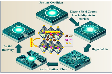
Metal halide perovskites have emerged as a game-changing class of semiconductors for next-generation light-emitting devices, thanks to their high photoluminescence quantum yields, tunable bandgaps, and low-cost solution processability. Perovskite light-emitting diodes (PeLEDs) are already demonstrating impressive brightness and color purity, making them strong candidates for future display and lighting technologies.
However, despite rapid performance gains, the long-term operational stability and reproducibility of PeLEDs remain critical challenges. These limitations are largely rooted in intrinsic factors like ion migration, trap-assisted recombination, and interface instability, which are still not fully understood.
At IIT Guwahati, our research group focuses on uncovering the fundamental physical mechanisms behind these limitations. We fabricate perovskite-based LEDs in our cleanroom and conduct comprehensive electrical and thermal characterizations, including:
-
Temperature-dependent impedance spectroscopy
-
Current–voltage analysis under bias stress
-
Deep-Level Transient Spectroscopy (DLTS)
These techniques allow us to probe how ions move, how traps evolve, and how the material and interfaces dynamically respond during device operation. Remarkably, we also investigate how the perovskite material exhibits self-healing behaviors, a phenomenon with significant implications for longevity.
By approaching PeLED research from an electronics and device physics perspective, our goal is to bridge the gap between material science and real-world device engineering. The insights gained from our studies contribute to a deeper understanding of perovskite device degradation and can inform strategies to design more stable, efficient, and scalable PeLEDs.
Device Modelling
Objective:
To understand the underlying physics of the different semiconductor devices which are simulated and fabricated experimentally in our laboratory, and derive analytical and semi-empirical models. For this purpose, we study and use advanced semiconductor characterization systems such as Deep Level Transient Spectroscopy, Impedance Spectroscopy and simulation tools like Santaurus TCAD, Silvaco, Matlab etc.
